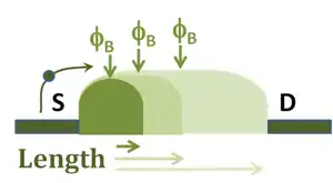
Drain-induced barrier lowering (DIBL) is a short-channel effect in MOSFETs referring originally to a reduction of threshold voltage of the transistor at higher drain voltages. In a classic planar field-effect transistor with a long channel, the bottleneck in channel formation occurs far enough from the drain contact that it is electrostatically shielded from the drain by the combination of the substrate and gate, and so classically the threshold voltage was independent of drain voltage. In short-channel devices this is no longer true: The drain is close enough to gate the channel, and so a high drain voltage can open the bottleneck and turn on the transistor prematurely.
The origin of the threshold decrease can be understood as a consequence of charge neutrality: the Yau charge-sharing model. [1] The combined charge in the depletion region of the device and that in the channel of the device is balanced by three electrode charges: the gate, the source and the drain. As drain voltage is increased, the depletion region of the p-n junction between the drain and body increases in size and extends under the gate, so the drain assumes a greater portion of the burden of balancing depletion region charge, leaving a smaller burden for the gate. As a result, the charge present on the gate retains charge balance by attracting more carriers into the channel, an effect equivalent to lowering the threshold voltage of the device.
In effect, the channel becomes more attractive for electrons. In other words, the potential energy barrier for electrons in the channel is lowered. Hence the term "barrier lowering" is used to describe these phenomena. Unfortunately, it is not easy to come up with accurate analytical results using the barrier lowering concept.
Barrier lowering increases as channel length is reduced, even at zero applied drain bias, because the source and drain form pn junctions with the body, and so have associated built-in depletion layers associated with them that become significant partners in charge balance at short channel lengths, even with no reverse bias applied to increase depletion widths.
The term DIBL has expanded beyond the notion of simple threshold adjustment, however, and refers to a number of drain-voltage effects upon MOSFET I-V curves that go beyond description in terms of simple threshold voltage changes, as described below.
As channel length is reduced, the effects of DIBL in the subthreshold region (weak inversion) show up initially as a simple translation of the subthreshold current vs. gate bias curve with change in drain-voltage, which can be modeled as a simple change in threshold voltage with drain bias. However, at shorter lengths the slope of the current vs. gate bias curve is reduced, that is, it requires a larger change in gate bias to effect the same change in drain current. At extremely short lengths, the gate entirely fails to turn the device off. These effects cannot be modeled as a threshold adjustment.[2]
DIBL also affects the current vs. drain bias curve in the active mode, causing the current to increase with drain bias, lowering the MOSFET output resistance. This increase is additional to the normal channel length modulation effect on output resistance, and cannot always be modeled as a threshold adjustment.
In practice, the DIBL can be calculated as follows:
where or Vtsat is the threshold voltage measured at a supply voltage (the high drain voltage), and or Vtlin is the threshold voltage measured at a very low drain voltage, typically 0.05 V or 0.1 V. is the supply voltage (the high drain voltage) and is the low drain voltage (for a linear part of device I-V characteristics). The minus in the front of the formula ensures a positive DIBL value. This is because the high drain threshold voltage, , is always smaller than the low drain threshold voltage, . Typical units of DIBL are mV/V.
DIBL can reduce the device operating frequency as well, as described by the following equation:
where is the supply voltage and is the threshold voltage.
References
- ↑ Narain Arora (2007). Mosfet Modeling for VLSI Simulation: Theory And Practice. World Scientific. p. 197, Fig. 5.14. ISBN 978-981-256-862-5.
- ↑ Yannis Tsividis (2003). Operation and Modeling of the MOS Transistor (Second ed.). New York: Oxford University Press. p. 268; Fig. 6.11. ISBN 0195170148.