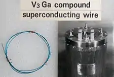
Superconducting wires are electrical wires made of superconductive material. When cooled below their transition temperatures, they have zero electrical resistance. Most commonly, conventional superconductors such as niobium–titanium are used,[1] but high-temperature superconductors such as YBCO are entering the market.
Superconducting wire's advantages over copper or aluminum include higher maximum current densities and zero power dissipation. Its disadvantages include the cost of refrigeration of the wires to superconducting temperatures (often requiring cryogens such as liquid nitrogen or liquid helium), the danger of the wire quenching (a sudden loss of superconductivity), the inferior mechanical properties of some superconductors, and the cost of wire materials and construction.[2]
Its main application is in superconducting magnets, which are used in scientific and medical equipment where high magnetic fields are necessary.
Important parameters
The construction and operating temperature will typically be chosen to maximise:
- Critical temperature Tc, the temperature below which the wire becomes a superconductor
- Critical current density Jc, the maximum current a superconducting wire can carry per unit cross-sectional area (see images below for examples with 20 kA/cm2).
Superconducting wires/tapes/cables usually consist of two key features:
- The superconducting compound (usually in the form of filaments/coating)
- A conduction stabilizer, which carries the current in case of the loss of superconductivity (known as quenching) in the superconductoring material.[3][4]
The current sharing temperature Tcs is the temperature at which the current transported through the superconductor also starts to flow through the stabilizer.[5][6] However, Tcs is not the same as the quench temperature (or critical temperature) Tc; in the former case, there is partial loss of superconductivity, while in the latter case, the superconductivity is entirely lost.[7]
LTS wire
Low-temperature superconductor (LTS) wires are made from superconductors with low critical temperature, such as Nb3Sn (niobium–tin) and NbTi (niobium–titanium). Often the superconductor is in filament form in a copper or aluminium matrix which carries the current should the superconductor quench for any reason. The superconductor filaments can form a third of the total volume of the wire.
Preparation
Wire drawing
The normal wire-drawing process can be used for malleable alloys such as niobium–titanium.
Surface diffusion
Vanadium–gallium (V3Ga) can be prepared by surface diffusion where the high temperature component as a solid is bathed in the other element as liquid or gas.[8] When all components remain in the solid state during high temperature diffusion this is known as the bronze process.[9]
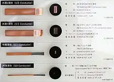 Cross sections of various (Nb,Ti)3Sn composite superconducting cables and wires. (440 to 7,800 A in 8 to 19 tesla fields).
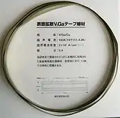 V3Ga superconducting tape (10×0.14 mm cross section). A vanadium core is covered with 15 µm V3Ga layer, then 20 µm bronze (stabilizing layer) and 15 µm insulating layer. Critical current 180 A (19.2 tesla, 4.2 K), critical current density 20 kA/cm2
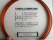 Nb/Cu-7.5at%Sn-0.4at%Ti tape (9.5×1.8 mm cross section) originally developed for an 18.1 T magnet. Nb core: 361×348 packs of 5 µm dia. filaments. Critical current 1700 A (16 tesla, 4.2 K), critical current density 20 kA/cm2
HTS wire
High-temperature superconductor (HTS) wires are made from superconductors with high critical temperature (high-temperature superconductivity), such as YBCO and BSCCO.
Powder-in-tube
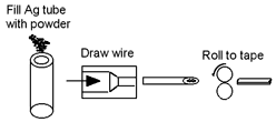
The powder-in-tube (PIT, or oxide powder in tube, OPIT) process is an extrusion process often used for making electrical conductors from brittle superconducting materials such as niobium–tin[10] or magnesium diboride,[11] and ceramic cuprate superconductors such as BSCCO.[12][13] It has been used to form wires of the iron pnictides.[14] (PIT is not used for yttrium barium copper oxide as it does not have the weak layers required to generate adequate 'texture' (alignment) in the PIT process.)
This process is used because the high-temperature superconductors are too brittle for normal wire forming processes. The tubes are metal, often silver. Often the tubes are heated to react the mix of powders. Once reacted the tubes are sometimes flattened to form a tape-like conductor. The resulting wire is not as flexible as conventional metal wire, but is sufficient for many applications.
There are in situ and ex situ variants of the process, as well a 'double core' method that combines both.[15]
Coated superconductor tape or wire
The coated superconductor tapes are known as second generation superconductor wires.[16] These wires are in a form of a metal tape of about 10 mm width and about 100 micrometer thickness, coated with superconductor materials such as YBCO. A few years after the discovery of High-temperature superconductivity materials such as the YBCO, it was demonstrated that epitaxial YBCO thin films grown on lattice matched single crystals such as magnesium oxide MgO, strontium titanate (SrTiO3) and sapphire had high supercritical current densities of 10–40 kA/mm2.[17][18] However, a lattice-matched flexible material was needed for producing a long tape. YBCO films deposited directly on metal substrate materials exhibit poor superconducting properties. It was demonstrated that a c-axis oriented yttria-stabilized zirconia (YSZ) intermediate layer on a metal substrate can yield YBCO films of higher quality, which had still one to two orders less critical current density than that produced on the single crystal substrates.[19][20]
The breakthrough came with the invention of ion beam-assisted deposition (IBAD) technique to produce of biaxially aligned yttria-stabilized zirconia (YSZ) thin films on metal tapes and the Rolling-Assisted-Biaxially-Textured-Substrates (RABiTS) process to produce biaxially textured metallic substrates via thermomechanically processing.[21][22]
In the IBAD process, the biaxially-textured YSZ film provided a single-crystal-like template for the epitaxial growth of the YBCO films. These YBCO films achieved critical current density of more than 1 MA/cm2. Other buffer layers such as cerium oxide (CeO2) and magnesium oxide (MgO) were produced using the IBAD technique for the superconductor films.[23][24] Details of the IBAD substrates and technology were reviewed by Arendt.[25] The process of LMO-enabled IBAD-MgO process was invented and developed at the Oak Ridge National Laboratory and won a R&D100 Award in 2007.[26] This LMO-enabled substrate process is now being used by essentially all manufacturers of HST wire based on the IBAD substrate. In the RABiTS substrates, the metallic template itself was biaxially-textured and heteroepitaxial buffer layers of Y2O3, YSZ and CeO2 were then deposited on the metallic template, followed by heterepitaxial deposition of the superconductor layer. Details of the RABiTS substrates and technology were reviewed by Goyal.[27]
As of 2015, YBCO coated superconductor tapes capable of carrying more than 500 A/cm-width at 77 K and 1000 A/cm-width at 30 K under high magnetic field have been demonstrated.[28][29][30][31] In 2021 YBCO coated superconductor tapes capable of carrying more than 250 A/cm-width at 77 K and 2500 A/cm-width at 20 K were reported for commercially produced wires.[32] In 2021 an experimental demonstration of an over-doped YBCO film reported 90 MA/cm2 at 5 K and 6 MA/cm2 at 77 K in a 7 T magnetic field.[33]
Metal organic chemical vapor deposition
Metal organic chemical vapor deposition (MOCVD) is one of the deposition processes used for fabrication of YBCO coated conductor tapes. Ignatiev provides an overview of MOCVD processes used to deposit YBCO films via MOCVD deposition.[34]
Reactive co-evaporation
Superconducting layer in the 2nd generation superconducting wires can also be grown by thermal evaporation of constituent metals, rare-earth element, barium, and copper. Prusseit provides an overview of the thermal evaporation process used to deposit high-quality YBCO films.[35]
Pulsed laser deposition
Superconducting layer in the 2nd generation superconducting wires can also be grown by pulsed laser deposition (PLD). Christen provides an overview of the PLD process used to deposit high-quality YBCO films.[36]
Standards
There are several IEC (International Electrotechnical Commission) standards related to superconducting wires under TC90.
See also
References
- ↑ "Characteristics of Superconducting Magnets". Superconductivity Basics. American Magnetics Inc. 2008. Retrieved October 11, 2008.
- ↑ Dumé, Belle (July 26, 2006). "Superconducting wire breaks record". Physics World. Archived from the original on October 30, 2007. Retrieved September 3, 2009.
- ↑ Wilson, Martin N. "Superconducting magnets." (1983).
- ↑ "Unit 4: Practical superconductors for accelerator magnets" (PDF).
- ↑ Bottura, L. "Magnet quench 101." arXiv preprint arXiv:1401.3927 (2014).
- ↑ Cutillas, Trueba; Manuel, Jose (September 20, 2017). "Effective field in large size superconducting cables for fusion".
- ↑ Ekin, Jack. Experimental techniques for low-temperature measurements: cryostat design, material properties and superconductor critical-current testing. Oxford university press, 2006.
- ↑ Matsushita, Teruo; Kikitsu, Akira; Sakata, Haruhisa; Yamafuji, Kaoru; Nagata, Masayuki (1986). "Elementary Pinning Force of Grain Boundaries in Superconducting V3Ga Tapes". Japanese Journal of Applied Physics. 25 (9): L792. Bibcode:1986JaJAP..25L.792M. doi:10.1143/JJAP.25.L792. S2CID 98297536.
- ↑ Dew-Hughes, D. (1978). "Solid-state (bronze process) V3Ga from a V-Al alloy core". Journal of Applied Physics. 49 (1): 327–332. Bibcode:1978JAP....49..327D. doi:10.1063/1.324390.
- ↑ Lindenhovius, J.L.H.; Hornsveld, E.M.; Den Ouden, A.; Wessel, W.A.J.; Ten Kate, H.H.J. (2000). "Powder-in-tube (PIT) Nb/sub 3/Sn conductors for high-field magnets" (PDF). IEEE Transactions on Applied Superconductivity. 10 (1): 975–978. Bibcode:2000ITAS...10..975L. doi:10.1109/77.828394. S2CID 26260700.
- ↑ Glowacki, B.A; Majoros, M; Vickers, M.E; Zeimetz, B (2001). "Superconducting properties of the powder-in-tube Cu-Mg-B and Ag-Mg-B wires". Physica C: Superconductivity. 372–376: 1254–1257. arXiv:cond-mat/0109085. Bibcode:2002PhyC..372.1254G. doi:10.1016/S0921-4534(02)00986-3. S2CID 119339527.
- ↑ Larbalestier, David et al. (1997) Ch. 5 "Sheathed or Powder-in-Tube Conductors" in WTEC Panel Report on Power Applications of Superconductivity in Japan and Germany
- ↑ Beales, Timothy P.; Jutson, Jo; Le Lay, Luc; Mölgg, Michelé (1997). "Comparison of the powder-in-tube processing properties of two (Bi2−xPbx)Sr2Ca2Cu 3O10+δ powders". Journal of Materials Chemistry. 7 (4): 653. doi:10.1039/a606896k.
- ↑ Ma, Y.; et al. (2009). "Fabrication and characterization of iron pnictide wires and bulk materials through the powder-in-tube method". Physica C. 469 (9–12): 651–656. arXiv:0906.3114. Bibcode:2009PhyC..469..651M. doi:10.1016/j.physc.2009.03.024. S2CID 118367961.
- ↑ Nakane, T.; Takahashi, K.; Kitaguchi, H.; Kumakura, H. (2009). "Fabrication of Cu-sheathed MgB2 wire with high Jc–B performance using a mixture of in situ and ex situ PIT techniques". Physica C: Superconductivity. 469 (15–20): 1531–1535. Bibcode:2009PhyC..469.1531N. doi:10.1016/j.physc.2009.05.227.
- ↑ Goyal, Amit. Second-Generation HTS Conductors. Springer New York, NY, 2005, https://doi.org/10.1007/b106635, Hardcover ISBN 978-1-4020-8117-0.
- ↑
Blue, C., & Boolchand, P. (1991). "In situ preparation of superconducting Y1Ba2Cu3O7−δ thin films by on-axis rf magnetron sputtering from a stoichiometric target". Applied Physics Letters. 58 (18): 2036. Bibcode:1991ApPhL..58.2036B. doi:10.1063/1.105005.
{{cite journal}}: CS1 maint: multiple names: authors list (link) - ↑
Savvides, N., & Katsaros, A. (1993). "In situ growth of epitaxial YBa2Cu3O7 thin films by on-axis unbalanced direct current magnetron sputtering". Applied Physics Letters. 62 (5): 528. Bibcode:1993ApPhL..62..528S. doi:10.1063/1.108901.
{{cite journal}}: CS1 maint: multiple names: authors list (link) - ↑
Russo, R. E., Reade, R. P., McMillan, J. M., & Olsen, B. L. (1990). "Metal buffer layers and Y-Ba-Cu-O thin films on Pt and stainless steel using pulsed laser deposition". Journal of Applied Physics. 68 (3): 1354. Bibcode:1990JAP....68.1354R. doi:10.1063/1.346681.
{{cite journal}}: CS1 maint: multiple names: authors list (link) - ↑
Reade, R. P., Berdahl, P., Russo, R. E., & Garrison, S. M. Laser (1992). "deposition of biaxially textured yttria-stabilized zirconia buffer layers on polycrystalline metallic alloys for high critical current Y-Ba-Cu-O thin films". Applied Physics Letters. 61 (18): 2231. Bibcode:1992ApPhL..61.2231R. doi:10.1063/1.108277.
{{cite journal}}: CS1 maint: multiple names: authors list (link) - ↑
Iijima, Y.; Tanabe, N.; Kohno, O.; Ikeno, Y. (1992). "In-plane aligned YBa2Cu3O7−x thin films deposited on polycrystalline metallic substrates". Applied Physics Letters. 60 (6): 769. Bibcode:1992ApPhL..60..769I. doi:10.1063/1.106514.
{{cite journal}}: CS1 maint: multiple names: authors list (link) - ↑ Goyal; et al. (1996). "High critical current density superconducting tapes by epitaxial deposition of YBa2Cu3Ox thick films on biaxially textured metals". Applied Physics Letters. 69 (12): 1795. Bibcode:1996ApPhL..69.1795G. doi:10.1063/1.117489.
- ↑
Gnanarajan, S., Katsaros, A., & Savvides, N. (1997). "Biaxially aligned buffer layers of cerium oxide, yttria stabilized zirconia, and their bilayers". Applied Physics Letters. 70 (21): 2816. Bibcode:1997ApPhL..70.2816G. doi:10.1063/1.119017.
{{cite journal}}: CS1 maint: multiple names: authors list (link) - ↑
Wang, C. P., Do, K. B., Beasley, M. R., Geballe, T. H., & Hammond, R. H (1997). "Deposition of in-plane textured MgO on amorphous Si3N4 substrates by ion-beam-assisted deposition and comparisons with ion-beam-assisted deposited yttria-stabilized-zirconia". Applied Physics Letters. 71 (20): 2955. Bibcode:1997ApPhL..71.2955W. doi:10.1063/1.120227.
{{cite journal}}: CS1 maint: multiple names: authors list (link) - ↑ Paul Arendt, Chapter 1 titled "IBAD Template Films for Coated Conductors", pages 3-28in Book titled Second-Generation HTS Conductors, edited by Goyal, Amit. Springer New York, NY, 2005, https://doi.org/10.1007/b106635, Hardcover ISBN 978-1-4020-8117-0.
- ↑ "ORNL wins six R&D 100 Awards, pushing total to 134 | ORNL".
- ↑ Amit Goyal, Chapter 2 titled "Epitaxial Superconductors on Rolling-Assisted-Biaxially-Textured-Substrates (RABiTS)", pages 29-46 in Book titled Second-Generation HTS Conductors, edited by Goyal, Amit. Springer New York, NY, 2005, https://doi.org/10.1007/b106635, Hardcover ISBN 978-1-4020-8117-0.
- ↑ Foltyn, S.R.; Arendt, P.N.; Dowden, P.C.; Depaula, R.F.; Groves, J.R.; Coulter, J.Y.; Quanxi Jia; Maley, M.P.; Peterson, D.E. (1999). "High-Tc coated conductors-performance of meter-long YBCO/IBAD flexible tapes". IEEE Transactions on Applied Superconductivity. 9 (2): 1519. Bibcode:1999ITAS....9.1519F. doi:10.1109/77.784682. S2CID 8640817.
- ↑ Usoskin, A., & Freyhardt, H. C. (2011). "YBCO-Coated Conductors Manufactured by High-Rate Pulsed Laser Deposition". MRS Bulletin. 29 (8): 583–589. doi:10.1557/mrs2004.165. S2CID 137126501.
{{cite journal}}: CS1 maint: multiple names: authors list (link) - ↑ Pahlke, Patrick; Hering, Michael; Sieger, Max; Lao, Mayraluna; Eisterer, Michael; Usoskin, Alexander; Stromer, Jan; Holzapfel, Bernhard; Schultz, Ludwig; Huhne, Ruben (2015). "Thick High Jc YBCO Films on ABAD-YSZ Templates". IEEE Transactions on Applied Superconductivity. 25 (3): 1. Bibcode:2015ITAS...2578533P. doi:10.1109/TASC.2014.2378533. S2CID 30199901.
- ↑ Selvamanickam, V., Gharahcheshmeh, M. H., Xu, A., Zhang, Y., & Galstyan, E. (2015). "Critical current density above 15 MA cm−2 at 30 K, 3 T in 2.2 μm thick heavily-doped (Gd,Y)Ba2Cu3Ox superconductor tapes". Superconductor Science and Technology. 28 (7): 072002. Bibcode:2015SuScT..28g2002S. doi:10.1088/0953-2048/28/7/072002. S2CID 123093286.
{{cite journal}}: CS1 maint: multiple names: authors list (link) - ↑ Molodyk, A.; Samoilenkov, S.; Markelov, A.; Degtyarenko, P.; Lee, S.; Petrykin, V.; Gaifullin, M.; Mankevich, A.; Vavilov, A.; Sorbom, B.; Cheng, J. (January 22, 2021). "Development and large volume production of extremely high current density YBa2Cu3O7 superconducting wires for fusion". Scientific Reports. 11 (1): 2084. doi:10.1038/s41598-021-81559-z. ISSN 2045-2322. PMC 7822827. PMID 33483553.
- ↑ Stangl, A.; Palau, A.; Deutscher, G.; Obradors, X.; Puig, T. (April 14, 2021). "Ultra-high critical current densities of superconducting YBa2Cu3O7-δ thin films in the overdoped state". Scientific Reports. 11 (1): 8176. arXiv:2009.03366. Bibcode:2021NatSR..11.8176S. doi:10.1038/s41598-021-87639-4. ISSN 2045-2322. PMC 8047038. PMID 33854183.
- ↑ Prusseit, W. (2005). Methods of HTS Deposition: Thermal Evaporation. In: Goyal, A. (eds) Second-Generation HTS Conductors. Springer, Boston, MA. https://doi.org/10.1007/0-387-25839-6_6.
- ↑ Prusseit, W. (2005). Methods of HTS Deposition: Thermal Evaporation. In: Goyal, A. (eds) Second-Generation HTS Conductors. Springer, Boston, MA. https://doi.org/10.1007/0-387-25839-6_6.
- ↑ Christen, H.M. (2005). Pulsed Laser Deposition of YBa2Cu2O7−δ for Coated Conductor Applications: Current Status and Cost Issues. In: Goyal, A. (eds) Second-Generation HTS Conductors. Springer, Boston, MA. https://doi.org/10.1007/0-387-25839-6_5.
